Hardware Guide
Types of Qubits
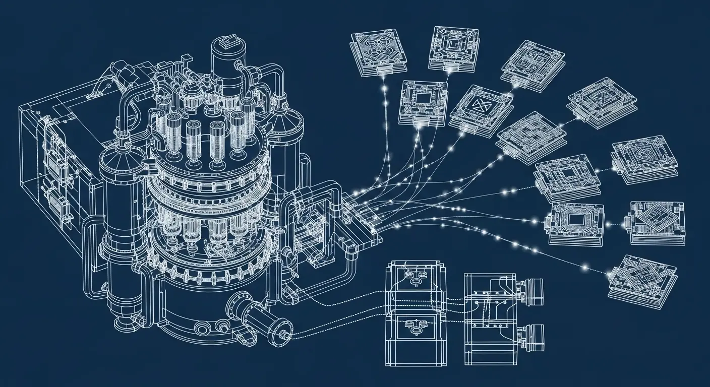
Every quantum computer uses a different physical system to encode quantum information. Here is how each approach works, who builds them, and what trade-offs they make.
At a Glance
| Type | Temperature | Gate Time | Coherence | Connectivity | Maturity | Key Players |
|---|---|---|---|---|---|---|
| Superconducting | ~15 millikelvin | 10–100 ns | 100–500 µs | Nearest-neighbour | IBM, Google | |
| Trapped Ion | Room temperature (ion trap itself) | 1–100 µs | Seconds to minutes | All-to-all | IonQ, Quantinuum | |
| Photonic | Room temperature (chip) | Picoseconds (optical) | Effectively infinite (photons do not decohere) | Configurable | Xanadu, PsiQuantum | |
| Neutral Atom | Room temperature (atom traps) | 0.1–10 µs | 1–10 seconds | Reconfigurable; | QuEra, Pasqal | |
| Silicon Spin | ~1 Kelvin | 1–100 ns | 1–100 ms | Nearest-neighbour | Intel, Quantum Motion | |
| Topological | ~15 millikelvin | Unknown (experimental stage) | Theoretically very long (topologically protected) | Unknown | Microsoft | |
| NV Center (Diamond) | Room temperature | ~10 ns | ~1 ms (at room temp), seconds (cryogenic) | Limited; | Quantum Brilliance, SaxonQ |
Superconducting
The workhorse of the industry
- Temperature
- ~15 millikelvin
- Gate time
- 10–100 ns
- Coherence
- 100–500 µs
- Connectivity
- Nearest-neighbour (grid or heavy-hex)
- Scalability
- High; established fab processes
How it works
Superconducting qubits are tiny circuits made from aluminium or niobium cooled to near absolute zero. Below a critical temperature the metal becomes superconducting (zero resistance). A Josephson junction, a nanoscale weak link in the circuit, creates a nonlinear inductance that gives the circuit an anharmonic energy spectrum. This means the ground state |0⟩ and first excited state |1⟩ can be addressed without accidentally driving higher levels. Microwave pulses at specific frequencies drive transitions between |0⟩ and |1⟩.
Advantages
- Fast gate operations (nanoseconds)
- Established semiconductor fabrication
- Largest single-chip qubit counts demonstrated to date (1,000+)
- Strong industrial investment
Challenges
- Requires dilution refrigerator at 15 mK
- Short coherence times vs trapped ions
- Limited qubit-to-qubit connectivity
- Fabrication variability between chips
Trapped Ion
Highest fidelity gates available today
- Temperature
- Room temperature (ion trap itself)
- Gate time
- 1–100 µs
- Coherence
- Seconds to minutes
- Connectivity
- All-to-all (any qubit can interact with any other)
- Scalability
- Moderate; scaling requires multi-trap architectures
How it works
Individual atoms are ionised (an electron is removed) and suspended in free space using electric fields. A radiofrequency or static electric field creates a potential well (the Paul trap) that holds the ions in a chain. Laser pulses or microwave radiation drive transitions between the electronic energy levels of the ion, which act as |0⟩ and |1⟩. Two-qubit gates are performed via the shared motional modes of the ion chain: exciting the motion of one ion vibrates the whole chain, coupling it to a neighbour.
Advantages
- Highest gate fidelities (~99.9% two-qubit)
- All-to-all connectivity; no SWAP overhead
- Long coherence times (seconds)
- Identical qubits by nature (same ion species)
Challenges
- Slow gate times (microseconds)
- Complex laser or microwave control systems
- Scaling to hundreds of qubits is hard
- Sensitive to vibration
Photonic
Quantum computing with light
- Temperature
- Room temperature (chip)
- Gate time
- Picoseconds (optical)
- Coherence
- Effectively infinite (photons do not decohere)
- Connectivity
- Configurable via beamsplitters and waveguides
- Scalability
- High potential; uses silicon photonics fabrication
How it works
Photons (particles of light) carry quantum information in their polarisation, time-bin, or path. Optical components (beamsplitters, phase shifters, waveguides) manipulate the quantum state. Single-photon sources inject photons one at a time; single-photon detectors read them out. Two-photon entanglement relies on photon bunching at beamsplitters (Hong-Ou-Mandel effect). Xanadu uses a continuous-variable approach with squeezed light rather than individual photons.
Advantages
- Photons do not decohere; they just get lost
- Natural for quantum networking and communication
- Room-temperature operation for the chip itself
- Silicon photonics is a mature manufacturing base
Challenges
- Photon loss is a major challenge
- Deterministic two-photon gates are hard
- Measurement is destructive
- Requires cryogenics for best single-photon detectors
Neutral Atom
Programmable arrays of thousands of atoms
- Temperature
- Room temperature (atom traps)
- Gate time
- 0.1–10 µs
- Coherence
- 1–10 seconds
- Connectivity
- Reconfigurable; atoms can be moved
- Scalability
- Very high potential; thousands of atoms demonstrated
How it works
Neutral atoms are cooled with lasers to microkelvin temperatures and trapped in arrays of optical tweezers (tightly focused laser beams). Each tweezer holds a single atom. The atomic ground and hyperfine states encode |0⟩ and |1⟩. Qubit interactions use Rydberg excitation: laser pulses promote atoms to high-energy Rydberg states where they have huge electric dipole moments and interact strongly with neighbouring atoms. This enables two-qubit gates via Rydberg blockade.
Advantages
- Thousands of qubits demonstrated in 2D arrays
- Reconfigurable connectivity; move atoms physically
- Long coherence times
- Good uniformity (identical atoms)
Challenges
- Two-qubit gates via Rydberg blockade have limited range
- Gate fidelities still improving (currently ~99%)
- Atom loss means qubit loss
- Requires ultra-high vacuum and laser cooling
Silicon Spin
Qubits in the same material as classical chips
- Temperature
- ~1 Kelvin
- Gate time
- 1–100 ns
- Coherence
- 1–100 ms
- Connectivity
- Nearest-neighbour (limited at present)
- Scalability
- Potentially very high; compatible with CMOS fabrication
How it works
An electron (or hole) is trapped in a quantum dot, a tiny region of a semiconductor defined by electrostatic gates. The spin of the electron (up = |0⟩, down = |1⟩) is the qubit. Microwave or magnetic field pulses manipulate the spin state. Two-qubit gates couple spins via exchange interaction: when two quantum dots are brought close, electrons can tunnel between them and their spins interact. Intel uses 300mm wafer fab; academic groups often use isotopically purified Si-28 to reduce magnetic noise from Si-29 nuclei.
Advantages
- Compatible with existing CMOS fab processes
- Tiny qubit size; potential for extreme density
- Less extreme cooling than superconducting (1 K vs 15 mK)
- Long coherence times in isotopically purified silicon
Challenges
- Still early stage, small qubit counts
- Individual qubit control is technically demanding
- Fabrication variability between qubits
- Limited two-qubit gate demonstrations at scale
Topological
Qubits protected by physics, not error correction
- Temperature
- ~15 millikelvin
- Gate time
- Unknown (experimental stage)
- Coherence
- Theoretically very long (topologically protected)
- Connectivity
- Unknown (architecture not yet demonstrated)
- Scalability
- High if realised; intrinsic error protection
How it works
Topological qubits encode quantum information in the global properties of a quantum system rather than in a single particle. The leading candidate uses Majorana zero modes: exotic quasiparticles that appear at the ends of semiconductor nanowires proximitised to superconductors (InAs/Al heterostructure). Because the information is stored non-locally, local noise cannot disturb the qubit state without correlating events at both ends simultaneously. Microsoft announced Majorana 1, a chip designed to hold 8 topological qubits, in February 2025; the claim that it realises true topological qubits is still being scrutinised by the research community. As of early 2026 the device is in active testing. The company targets scaling to a million qubits on a single chip, arguing that topological protection reduces the error correction overhead that limits other approaches.
Advantages
- Topological protection could give intrinsically low error rates
- Far fewer physical qubits needed per logical qubit
- Potential path to fault tolerance at smaller scale
Challenges
- Early stage: Microsoft Majorana 1 (announced Feb 2025) is a research prototype under active testing
- Gate fidelity data not yet publicly comparable to other platforms
- Timeline to practical scale remains uncertain
- Complex semiconductor/superconductor materials science challenges
NV Center (Diamond)
Qubits that work at room temperature
- Temperature
- Room temperature
- Gate time
- ~10 ns
- Coherence
- ~1 ms (at room temp), seconds (cryogenic)
- Connectivity
- Limited; small clusters
- Scalability
- Low at present; hard to scale
How it works
A nitrogen-vacancy (NV) centre is a point defect in diamond: a nitrogen atom next to a missing carbon atom (vacancy). The electron spin of this defect acts as a qubit. Crucially, the spin state can be initialised and read out with green laser light and a red photon, and manipulated with microwave pulses. Diamond's rigid crystal lattice protects the spin from noise, giving relatively long coherence times even at room temperature. The nuclear spin of the nitrogen atom can act as a second qubit with even longer coherence.
Advantages
- Operates at room temperature
- Natural interface with visible light; useful for sensing
- Good coherence for room-temperature operation
- Strong candidate for quantum network nodes
Challenges
- Hard to manufacture reproducibly
- Limited scaling beyond small numbers of qubits
- Two-qubit gates are slow and lower fidelity
- Not competitive with superconducting or trapped ion for computation